Fundamentals of Device and Systems Packaging: Technologies and Applications, Second Edition

Specificaties
Gebonden, blz. | Engels
McGraw-Hill Education | 2e druk, 2019
ISBN13: 9781259861550
Rubricering
McGraw-Hill Education 2e druk, 2019 9781259861550
Verwachte levertijd ongeveer 11 werkdagen

Samenvatting

Publisher's Note: Products purchased from Third Party sellers are not guaranteed by the publisher for quality,  authenticity, or access to any online entitlements included with the product.

A fully updated, comprehensive guide to microelectronic device and systems packaging principles and practices

This thoroughly revised book offers the latest, comprehensive fundamentals in device and systems packaging technologies and applications. You will get in-depth explanations of the 15 core packaging technologies that make up any electronic system, including electrical design for power, signal, and EMI; thermal design by conduction, convection,and radiation heat transfer; thermo-mechanical failures and reliability;advanced packaging materials at micro and nanoscales; ceramic, organic, glass,and silicon substrates. This resource also discusses passive components such as capacitors, inductors, and resistors and their proximity integration with actives; chip-to-package interconnections and assembly; wafer and panel embedding technologies; 3D packaging with and without TS; RF and millimeter-wave packaging; role of optoelectronics; mems and sensor packaging;encapsulation, molding and sealing; and printed wiring board and its assembly to form end-product systems. 

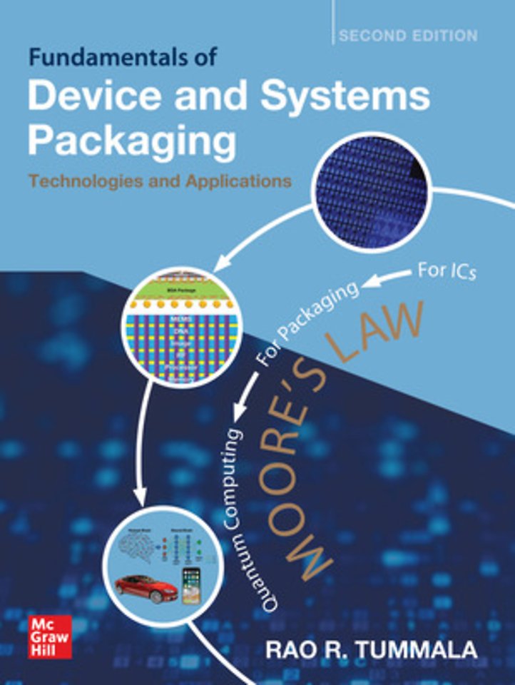
Fundamentals of Device and Systems Packaging: Technologies and Applications, Second Edition introduces the concept of Moore’s Law for packaging, as Moore’s Law for ICs is coming to an end due to physical, material, electrical, and financial limitations. Moore’s Law for Packaging (MLP) can be viewed as interconnecting and integrating many smaller chips with high aggregate transistor density, at higher performance and lower cost than Moore’s Law for ICs. This book lays the groundwork for Moore’s Law for Packaging by showing how I/Os have evolved from one package family node to the next, starting with

Specificaties

ISBN13:9781259861550
Taal:Engels
Bindwijze:gebonden
Druk:2

Inhoudsopgave

Preface <br/> 1 Introduction to Device and Systems Packaging Technologies <br/> 1.1 What Is Packaging and Why? <br/> 1.1.1 What Is Packaging? <br/> 1.1.2 Why Is Packaging Important? <br/> 1.1.3 Every IC and Device Has to Be Packaged <br/> 1.1.4 Controls Performance of Computers <br/> 1.1.5 Controls Size of Consumer Electronics <br/> 1.1.6 Controls Reliability of Electronics <br/> 1.1.7 Controls Cost of Electronic Products <br/> 1.1.8 Required in Nearly Everything <br/> 1.2 Anatomy of an Electronic Packaged System from a Packaging Point of View <br/> 1.2.1 Fundamentals of Packaging <br/> 1.2.2 Systems Packaging Involves Electrical, Mechanical, and Materials Technologies <br/> 1.2.3 Nomenclature <br/> 1.3 Devices and Moore’s Law <br/> 1.3.1 On-Chip Interconnections <br/> 1.3.2 Interconnect Materials <br/> 1.3.3 The Resistance and Capacitance Delays (RC Delays) of On-Chip Interconnects <br/> 1.3.4 Future of Device Scaling <br/> 1.4 Electronic Technology Waves: Microelectronics, RF/Wireless, Photonics, MEMS, and Quantum Devices <br/> 1.4.1 Microelectronics: The First Technology Wave <br/> 1.4.2 RF and Wireless: The Second Technology Wave <br/> 1.4.3 Photonics: The Third Technology Wave <br/> 1.4.4 Micro-Electro-Mechanical Systems (MEMS): The Fourth Technology Wave <br/> 1.4.5 Quantum Devices and Computing: Fifth Wave <br/> 1.5 Packaging and Moore’s Law for Packaging <br/> 1.5.1 Three Eras in Packaging <br/> 1.5.2 Moore’s Law or SOC Era (1960–2010) <br/> 1.5.3 Moore’s Law for Packaging Era from 2010 to 2025 <br/> 1.5.4 Moore’s Law for Systems Era from 2025 <br/> 1.6 Electronic Systems Technologies Trends <br/> 1.6.1 Core Packaging Technologies <br/> 1.6.2 Packaging Technologies and Their Trends <br/> 1.7 Future Outlook <br/> 1.7.1 Emerging Computing Systems <br/> 1.7.2 Emerging 3D Systems Packaging <br/> 1.8 How the Book Is Organized <br/> 1.9 Homework Problems <br/> 1.10 Suggested Reading <br/> Part 1 Fundamentals of Packaging <br/> 2 Fundamentals of Electrical Design for Signals, Power, and Electromagnetic Interference <br/> 2.1 What Is Electrical Package Design and Why? <br/> 2.2 Electrical Anatomy of a Package <br/> 2.2.1 Fundamentals of Electrical Package Design <br/> 2.2.2 Nomenclature <br/> 2.3 Signal Distribution <br/> 2.3.1 Devices and Interconnections <br/> 2.3.2 Kirchhoff’s Laws and Transit Time Delay <br/> 2.3.3 Transmission Line Behavior of Interconnections <br/> 2.3.4 Characteristic Impedance <br/> 2.3.5 Typical Transmission Line Structures Used as Package Interconnections <br/> 2.3.6 Transmission Line Losses <br/> 2.3.7 Crosstalk <br/> 2.4 Power Distribution <br/> 2.4.1 Power Supply Noise <br/> 2.4.2 Inductive Effects <br/> 2.4.3 Effective Inductance <br/> 2.4.4 Effect of Package Design on Inductance <br/> 2.4.5 Decoupling Capacitors <br/> 2.5 Electromagnetic Interference <br/> 2.6 Summary and Future Trends <br/> 2.7 Homework Problems <br/> 2.8 Suggested Reading <br/> 3 Fundamentals of Thermal Technologies <br/> 3.1 What Is Thermal Management and Why? <br/> 3.2 Anatomy of a Thermal Package System <br/> 3.2.1 Fundamentals of Heat Transfer <br/> 3.2.2 Nomenclature <br/> 3.3 Chip Level Thermal Technologies <br/> 3.3.1 Thermal Interface Materials (TIMs) <br/> 3.3.2 Heat Spreaders <br/> 3.3.3 Thermal Vias <br/> 3.4 Module Level Thermal Technologies <br/> 3.4.1 Heat Sinks <br/> 3.4.2 Heat Pipes and Vapor Chambers <br/> 3.4.3 Closed-Loop Liquid Cooling <br/> 3.4.4 Cold Plates <br/> 3.4.5 Immersion Cooling <br/> 3.4.6 Jet Impingement Cooling <br/> 3.4.7 Spray Cooling <br/> 3.5 System Level Thermal Technologies <br/> 3.5.1 Air Cooling <br/> 3.5.2 Hybrid Cooling <br/> 3.5.3 Immersion Cooling <br/> 3.6 Power and Cooling Technologies for Electric Vehicles <br/> 3.7 Summary and Future Trends <br/> 3.8 Homework Problems <br/> 3.9 Suggested Reading <br/> 4 Fundamentals of Thermo-Mechanical Reliability <br/> 4.1 What Is Thermo-Mechanical Reliability? <br/> 4.2 Anatomy of a Package with Failures and Failure Mechanisms <br/> 4.2.1 Fundamentals of Thermo-Mechanical Reliability <br/> 4.2.2 Thermo-Mechanical Modeling <br/> 4.2.3 Nomenclature <br/> 4.3 Types of Thermo-Mechanical-Induced Failures and Design Guidelines for Reliability <br/> 4.3.1 Fatigue Failures <br/> 4.3.2 Brittle Fractures <br/> 4.3.3 Creep-Induced Failures <br/> 4.3.4 Delamination-Induced Failures <br/> 4.3.5 Plastic Deformation Failures <br/> 4.3.6 Warpage-Induced Failures <br/> 4.4 Summary and Future Trends <br/> 4.5 Homework Problems <br/> 4.6 Suggested Reading <br/> 5 Fundamentals of Package Materials at Microscale and Nanoscale <br/> 5.1 What Is the Role of Materials in Packaging? <br/> 5.2 Anatomy of a Package with a Variety of Materials <br/> 5.2.1 Fundamentals of Package Materials <br/> 5.2.2 Nomenclature <br/> 5.3 Package Materials, Processes, and Properties <br/> 5.3.1 Substrate Materials, Processes, and Properties <br/> 5.3.2 Interconnection and Assembly Materials, Processes, and Properties <br/> 5.3.3 Passive Component Materials, Processes, and Properties <br/> 5.3.4 Thermal and Thermal Interface Materials (TIMs), Processes, and Properties <br/> 5.4 Summary and Future Trends <br/> 5.5 Homework Problems <br/> 5.6 Suggested Reading <br/> 6 Fundamentals of Ceramic, Organic, Glass, and Silicon Package Substrates <br/> 6.1 What Is a Package Substrate and Why? <br/> 6.2 Anatomy of Three Package Substrates: Ceramics, Organic Laminates, and Silicon <br/> 6.2.1 Fundamentals of Package Substrates <br/> 6.2.2 Nomenclature <br/> 6.3 Package Substrate Technologies <br/> 6.3.1 Historical Trends <br/> 6.4 Thick-Film Substrates <br/> 6.4.1 Ceramic Substrates <br/> 6.5 Thin-Film Substrates <br/> 6.5.1 Organic Substrates <br/> 6.5.2 Glass Substrates <br/> 6.6 Ultra-Thin-Film Substrates with Semiconductor Packaging Processes <br/> 6.6.1 Silicon Substrates <br/> 6.7 Summary and Future Trends <br/> 6.8 Homework Problems <br/> 6.9 Suggested Reading <br/> 7 Fundamentals of Passive Components and Integration with Active Devices <br/> 7.1 What Are Passive Components and Why? <br/> 7.2 Anatomy of Passive Components <br/> 7.2.1 Fundamentals of Passive Components <br/> 7.2.2 Nomenclature <br/> 7.3 Passive Component Technologies <br/> 7.3.1 Discrete Passives <br/> 7.3.2 Integrated Passive Devices (IPDs) <br/> 7.3.3 Embedded Discrete Passives <br/> 7.3.4 Embedded Thin-Film Passives <br/> 7.4 Functional Modules with Passives and Actives <br/> 7.4.1 RF Modules <br/> 7.4.2 Power Modules <br/> 7.4.3 Voltage Regulator Power Modules <br/> 7.5 Summary and Future Trends <br/> 7.6 Homework Problems <br/> 7.7 Suggested Reading <br/> 8 Fundamentals of Chip-to-Package Interconnections and Assembly <br/> 8.1 What Are Chip-to-Package Interconnections and Assembly and Why? <br/> 8.2 Anatomy of an Interconnection and Assembly <br/> 8.2.1 Types of Chip-Level Interconnections and Assembly Technologies <br/> 8.2.2 Fundamentals of Interconnections and Assembly <br/> 8.2.3 Fundamentals of Assembly and Bonding <br/> 8.2.4 Nomenclature <br/> 8.3 Interconnection and Assembly Technologies <br/> 8.3.1 Evolution <br/> 8.4 Interconnections and Assembly Technologies <br/> 8.4.1 Wire-Bonding <br/> 8.4.2 Tape Automated Bonding (TAB) <br/> 8.4.3 Flip-Chip Interconnection and Assembly Technology <br/> 8.4.4 Copper Pillar with Solder Cap Technology <br/> 8.4.5 SLID Interconnection and Assembly Technology <br/> 8.5 Future Trends in Interconnection and Assembly Technologies <br/> 8.5.1 Extension of SLID <br/> 8.6 Homework Problems <br/> 8.7 Suggested Reading <br/> 9 Fundamentals of Embedded and Fan-Out Packaging <br/> 9.1 What Is Embedding and Fan-Out Packaging and Why? <br/> 9.1.1 Why Embedding and Fan-Out Packaging? <br/> 9.2 Anatomy of a Fan-Out Wafer-Level Package (FO-WLP) <br/> 9.2.1 A Typical Fan-Out Wafer-Level Package Process <br/> 9.2.2 Fundamentals of Fan-Out Wafer-Level Package Technology <br/> 9.2.3 Nomenclature <br/> 9.3 Fan-Out Wafer-Level Package Technologies <br/> 9.3.1 Types <br/> 9.3.2 Materials and Processes <br/> 9.3.3 Fan-Out Wafer-Level Packaging Tools <br/> 9.3.4 Challenges in Fan-Out Wafer-Level Packaging Technology <br/> 9.3.5 Applications of Fan-Out Wafer-Level Packaging <br/> 9.4 Panel-Level Package (PLP) <br/> 9.4.1 What Is Panel-Level Packaging and Why? <br/> 9.4.2 Types of Manufacturing Infrastructure for Panel-Level Packaging <br/> 9.4.3 Applications of Panel-Level Packaging <br/> 9.5 Summary and Future Trends <br/> 9.6 Homework Problems <br/> 9.7 Suggested Reading <br/> 10 Fundamentals of 3D Packaging with and without TSV <br/> 10.1 What Are 3D ICs with TSV and Why? <br/> 10.1.1 Why 3D ICs with TSVs? <br/> 10.2 Anatomy of a 3D Package with TSV <br/> 10.2.1 Fundamentals of 3D ICs with TSV <br/> 10.2.2 Nomenclature <br/> 10.3 3D ICs with TSV Technologies <br/> 10.3.1 Through-Silicon-Vias (TSVs) <br/> 10.3.2 Ultra-Thin ICs <br/> 10.3.3 Back-End-of-Line (BEOL) RDL Wiring <br/> 10.3.4 Chip-to-Chip Interconnections within the 3D Stack <br/> 10.3.5 Packages for 3D IC Stacks <br/> 10.3.6 Underfill <br/> 10.4 Summary and Future Trends <br/> 10.5 Homework Problems <br/> 10.6 Suggested Reading <br/> 10.7 Acknowledgment <br/> 11 Fundamentals of RF and Millimeter-Wave Packaging <br/> 11.1 What Is RF and Why? <br/> 11.1.1 History and Evolution <br/> 11.1.2 When Was the First Mobile Phone Introduced? <br/> 11.2 Anatomy of an RF System <br/> 11.2.1 Fundamentals of RF <br/> 11.2.2 RF Nomenclature <br/> 11.3 RF Technologies and Applications <br/> 11.3.1 Transceiver <br/> 11.3.2 Transmitter <br/> 11.3.3 Receiver <br/> 11.3.4 Modulation Schemes <br/> 11.3.5 Antenna <br/> 11.3.6 Components in RF Front-End Module <br/> 11.3.7 Filters <br/> 11.3.8 RF Materials and Components <br/> 11.3.9 RF Modeling and Characterization Techniques <br/> 11.3.10 Applications of RF <br/> 11.4 What Is a Millimeter-Wave System? <br/> 11.5 Anatomy of a Millimeter-Wave Package <br/> 11.5.1 Fundamentals of Millimeter-Wave Packaging <br/> 11.6 Millimeter-Wave Technologies and Applications <br/> 11.6.1 5G and Beyond <br/>
11.6.2 Automotive Radars <br/> 11.6.3 Millimeter-Wave Imaging <br/> 11.7 Summary and Future Trends <br/> 11.8 Homework Problems <br/> 11.9 Suggested Reading <br/> 12 Fundamentals of Optoelectronics Packaging <br/> 12.1 What Is Optoelectronics? <br/> 12.2 Anatomy of an Optoelectronics System <br/> 12.2.1 Fundamentals of Optoelectronics <br/> 12.2.2 Nomenclature <br/> 12.3 Optoelectronic Technologies <br/> 12.3.1 Active Optoelectronic Devices <br/> 12.3.2 Passive Optical Devices <br/> 12.3.3 Optical Interconnections <br/> 12.4 Optoelectronic Systems, Applications, and Markets <br/> 12.4.1 Optoelectronic Systems <br/> 12.4.2 Applications of Optoelectronics <br/> 12.4.3 Optoelectronics Markets <br/> 12.5 Summary and Future Trends <br/> 12.6 Homework Problems <br/> 12.7 Suggested Reading <br/> 13 Fundamentals of MEMS and Sensor Packaging <br/> 13.1 What Are MEMS? <br/> 13.1.1 Historical Evolution <br/> 13.2 Anatomy of a MEMS Package <br/> 13.2.1 Fundamentals of MEMS Packaging <br/> 13.2.2 Nomenclature <br/> 13.3 MEMS and Sensor Device Fabrication Technologies <br/> 13.3.1 Photolithographic Pattern Transfer <br/> 13.3.2 Thin-Film Deposition <br/> 13.3.3 Wet and Dry Etching <br/> 13.3.4 Bulk and Surface Micromachining of Silicon <br/> 13.3.5 Wafer Bonding <br/> 13.3.6 Laser Micromachining <br/> 13.3.7 Process Integration <br/> 13.4 MEMS Packaging Technologies <br/> 13.4.1 MEMS Package Materials <br/> 13.4.2 MEMS Package Assembly Processes <br/> 13.5 Application of MEMS and Sensors <br/> 13.5.1 Pressure Sensors <br/> 13.5.2 Accelerometers and Gyroscopes <br/> 13.5.3 Projection Displays <br/> 13.6 Summary and Future Trends <br/> 13.7 Homework Problems <br/> 13.8 Suggested Reading <br/> 14 Fundamentals of Package Encapsulation, Molding, and Sealing <br/> 14.1 What Is Sealing and Encapsulation and Why? <br/> 14.2 Anatomy of an Encapsulated and a Sealed Package <br/> 14.2.1 Fundamentals of Encapsulation and Sealing <br/> 14.2.2 Nomenclature <br/> 14.3 Properties of Encapsulants <br/> 14.3.1 Mechanical Properties <br/> 14.3.2 Thermal Properties <br/> 14.3.3 Physical Properties <br/> 14.4 Encapsulation Materials <br/> 14.4.1 Epoxy and Related Materials <br/> 14.4.2 Cyanate Ester <br/> 14.4.3 Urethanes <br/> 14.4.4 Silicones <br/> 14.5 Encapsulation Processes <br/> 14.5.1 Molding <br/> 14.5.2 Liquid Encapsulation <br/> 14.6 Hermetic Sealing <br/> 14.6.1 Sealing Processes <br/> 14.7 Summary and Future Trends <br/> 14.8 Homework Problems <br/> 14.9 Suggested Reading <br/> 15 Fundamentals of Printed Wiring Boards <br/> 15.1 What Is a Printed Wiring Board? <br/> 15.2 Anatomy of a Printed Wiring Board <br/> 15.2.1 Fundamentals of Printed Wiring Boards <br/> 15.2.2 Types of PWBs <br/> 15.2.3 PWB Material Grades <br/> 15.2.4 Single- to Multi-Layer Boards and Their Applications <br/> 15.2.5 PWB Design Elements <br/> 15.2.6 Nomenclature <br/> 15.3 Printed Wiring Board Technologies <br/> 15.3.1 PWB Materials <br/> 15.3.2 PWB Fabrication <br/> 15.3.3 PWB Applications <br/> 15.4 Summary and Future Trends <br/> 15.5 Homework Problems <br/> 15.6 Suggested Reading <br/> 16 Fundamentals of Board Assembly <br/> 16.1 What Is a Printed Circuit Board Assembly (PCBA) and Why? <br/> 16.2 Anatomy of Printed Circuit Board Assembly <br/> 16.2.1 Fundamentals of PCBA <br/> 16.2.2 Nomenclature <br/> 16.3 PCBA Technologies <br/> 16.3.1 PCB Substrate <br/> 16.3.2 Package Substrates <br/> 16.4 Types of Printed Circuit Board Assembly <br/> 16.4.1 Plated Through Hole (PTH) Assembly <br/> 16.4.2 Surface Mount Assembly (SMA) <br/> 16.5 Types of Assembly Soldering Processes <br/> 16.5.1 Reflow Soldering <br/> 16.5.2 Wave Soldering with PTH <br/> 16.6 Summary and Future Trends <br/> 16.7 Homework Problems <br/> 16.8 Suggested Reading <br/> 16.9 Acknowledgment <br/> Part 2 Applications of Packaging Technologies <br/> 17 Applications of Packaging Technologies in Future Car Electronics <br/> 17.1 What Are Future Car Electronics and Why? <br/> 17.2 Anatomy of a Future Car <br/> 17.2.1 Fundamentals of a Future Car <br/> 17.2.2 Nomenclature <br/> 17.3 Future Car Electronic Technologies <br/> 17.3.1 Computing and Communications <br/> 17.3.2 Sensing Electronics <br/> 17.3.3 High-Power Electronics <br/> 17.4 Summary and Future Trends <br/> 17.5 Homework Problems <br/> 17.6 Suggested Reading <br/> 18 Applications of Packaging Technologies in Bioelectronics <br/> 18.1 What Are Bioelectronics? <br/> 18.1.1 Bioelectronics Applications <br/> 18.1.2 Anatomy of a Bioelectronic System <br/> 18.2 Packaging Technologies for Bioelectronic Systems <br/> 18.2.1 Biocompatible and Biostable Packaging <br/> 18.2.2 Heterogeneous Integration <br/> 18.3 Examples of Bioelectronic Implants <br/> 18.3.1 Pacemakers and Electronic Stents <br/> 18.3.2 Cochlear Implants <br/> 18.3.3 Retinal Prosthetics <br/> 18.3.4 Neuromuscular Stimulators <br/> 18.3.5 Brain Neural Recording and Stimulations <br/> 18.4 Summary and Future Trends <br/> 18.5 Homework Problems <br/> 18.6 Suggested Reading <br/> 19 Applications of Packaging Technologies in Communication Systems <br/> 19.1 What Are Communication Systems and Why? <br/> 19.2 Anatomy of Two Communication Systems: Wired and Wireless <br/> 19.2.1 Anatomy of a Wired Communication System <br/> 19.2.2 Anatomy of a Wireless Communication System <br/> 19.3 Communication System Technologies <br/> 19.3.1 Historical Evolution <br/> 19.3.2 Communication System Technologies <br/> 19.3.3 Wireless Communication System Technologies <br/> 19.4 Summary and Future Trends <br/> 19.5 Homework Problems <br/> 19.6 Suggested Reading <br/> 20 Applications of Packaging Technologies in Computing Systems <br/> 20.1 What Is Computer Packaging? <br/> 20.2 The Anatomy of a Computer Package <br/> 20.2.1 Fundamentals of Computer Packaging <br/> 20.2.2 Types of Computing Systems <br/> 20.2.3 Nomenclature <br/> 20.3 Computer Packaging Technologies <br/> 20.3.1 Evolution <br/> 20.3.2 Interconnection Technologies <br/> 20.3.3 Interconnection Designs for Signal and Power <br/> 20.4 Thermal Technologies <br/> 20.4.1 Thermal Management <br/> 20.4.2 Thermo-Mechanical Reliability <br/> 20.4.3 Material Technologies <br/> 20.5 Summary and Future Trends <br/> 20.5.1 Beginning of Moore’s Law for Packaging <br/> 20.5.2 Moore’s Law for Packaging: Cost <br/> 20.6 Homework Problems <br/> 20.7 Suggested Reading <br/> 20.8 Acknowledgments <br/> 21 Applications of Packaging Technologies in Flexible Electronics <br/> 21.1 What Are Flexible Electronics and Why? <br/> 21.1.1 Applications <br/> 21.2 Anatomy of a Flexible Electronic System <br/> 21.2.1 Fundamentals of Flexible Electronics Technologies <br/> 21.2.2 Nomenclature <br/> 21.3 Flexible Electronics Technologies <br/> 21.3.1 Component Technologies <br/> 21.3.2 Process Integration of Flexible Electronics Technologies <br/> 21.3.3 Component Assembly on Flexible Substrates <br/> 21.4 Summary and Future Trends <br/> 21.5 Homework Problems <br/> 21.6 Suggested Reading <br/> 22 Applications of Packaging Technologies in Smartphones <br/> 22.1 What Are Smartphones? <br/> 22.1.1 Why Smartphones? <br/> 22.1.2 Historical Evolution of Smartphones <br/> 22.2 Anatomy of a Smartphone <br/> 22.2.1 Fundamentals of Smartphones <br/> 22.2.2 Nomenclature <br/> 22.3 Smartphone Packaging Technologies <br/> 22.3.1 Application Processor Packaging <br/> 22.3.2 Memory Packaging <br/> 22.3.3 RF Packaging <br/> 22.3.4 Power Packaging <br/> 22.3.5 MEMS and Sensors Packaging <br/> 22.4 Systems Packaging in Smartphones <br/> 22.5 Summary and Future Trends <br/> 22.6 Homework Problems <br/> 22.7 Suggested Reading <br/> Index

Rubrieken

    Personen

      Trefwoorden

        Fundamentals of Device and Systems Packaging: Technologies and Applications, Second Edition